 All-in-One COB LED TV
  Flexible LED Displays
  Transparent LED Displays
  Led Poster
  Circular LED Displays
  Creative & Custom LED Displays
 As the LED technology matures, Mini LED backlight (abbreviated as Mini BLU) has become the most promising display technology in the HD display. The technology attract leading LED manufacturers in the upstream chips, midstream packaging and downstream display chain to enter the market. It also accelerate the commercialization of Mini BLU.
Among them, the LED packaging is the key link that determines the LED performance, yield cost and even large-scale production of Mini BLU products. The technical route of the best packaging solution has never stopped. So, the current focus is on the competition between POB and COB.
COB vs POB Packaging Tecnology
In traditional backlight LED solutions, SMD flip-chip packaging has dominated the LED encapsulation approach. As the industry enters the era of LED miniaturization, with the maturation of flip-chip technology, flip-chip SMD and COB packaging technologies have gradually emerged. The competition between the two major Mini LED is intensifying.
COB Packaging Technology:

COB involves mounting a large number of LED chips directly onto a substrate (primarily PCB or glass substrates) through die bonding, followed by integrated encapsulation.
COB technology adopts a highly integrated pixel-level panel packaging structure on one side of the substrate, while driver IC components are arranged on the reverse side. Due to eliminating the need for brackets or solder pins, COB enables an optical mixing distance (OD) approaching zero, allowing ultra-thin backlight module designs.
However, the COB process demands high precision and complex manufacturing, requiring advanced equipment compared to traditional POB workflows.
Additionally, the integrated encapsulation complicates rework for defective products.
However, COB solutions more expensive than POB due to some factors such as process complexity and equipment cost allocationetc.
POB Technology:
POB (Package-on-Board), commonly referred to as the “Starry Sky” solution in the industry. It involves encapsulating individual LED chips into discrete lamp beads first, which are then mounted onto the substrate via SMT. This fundamentally differs from the integrated approach of COB.
Key distinctions:
- COB: Direct chip-to-substrate bonding, integrated encapsulation, minimized OD, thinner modules, higher cost.
- POB: Pre-packaged discrete LEDs, SMT assembly, simpler process, lower cost, but thicker backlight design.
POB Flip-Chip SMD Package Structure Schematic

Currently, POB backlight solutions can be categorized into flip-chip SMD and CSP types based on package structure. The POB flip-chip SMD technology offers mature processes, relatively low costs, and strong mass production feasibility.
However, due to limitations in package size, it generally requires larger OD (Optical Distance) values, resulting in narrower application compared to COB solutions.
POB-CSP Package Structure Schematic

CSP (Chip Scale Package) is a chip-level packaging technology. The post-packaging volume is approximately 1.2 times the chip size. So, it enables ultra-small OD values comparable to COB solutions while maintaining lower costs than COB.
Nonetheless, the extremely compact size of CSP LEDs leads to challenges such as excessively narrow electrode pad spacing and insufficient pad area, which may cause light leakage, uneven color mixing, or optical crosstalk due to inadequate encapsulation resin coverage.
Comparison of COB vs POB Technologies
Currently, the two packaging solutions for Mini LED backlight units. COB and POB have distinct advantages and limitations, leading to their adoption in different products based on market demands.
Comparison Criteria COB POB
| Comparison Criteria | COB | POB |
|---|---|---|
| Industry Chain | Requires redevelopment and integration | Mature |
| Investment | High (requires secondary investments) | Low |
| Chip Type | Square wafer production | Mass-produced round wafers |
| Substrate Precision | High requirements | Low requirements |
| Rework Difficulty | High (complex process) | Low (manual rework possible) |
| Application Scenarios | Ultra-thin backlight (e.g., tablets, laptops, gaming displays) | Large-screen backlight (e.g., mid/low-tier TVs, monitors, automotive) |
Critical Analysis
Industry Chain:POB > COB
COB involves chip-level bonding, demanding higher technical standards for equipment, materials, and processes. Its supply chain maturity remains underdeveloped.
POB benefits from a mature supply chain. It enabe mass production without major upgrades to existing lines, significantly reducing costs.
Raw Materials:POB > COB
COB requires square wafers, which have stricter material specifications.
POB uses cost-effective round wafers produced at scale, supporting smaller chip sizes and lower costs.
Production Yield:Flip-Chip SMD > CSP > COB
COB demands ultra-high precision and quality control, resulting in lower module yields.
to ensure pass rates, It need additional processes:
- SPI for solder paste inspection
- AOI for visual inspection
- performance testing, aging
With PCB substrates, POB flip-chip SMD outperforms COB due to larger solder pads, mature processes, and looser substrate precision requirements. POB-CSP yields fall between flip-chip SMD and COB.
Rework Flexibility:POB > COB
COB’s integrated encapsulation complicates rework for defective units.
POB allows manual replacement of individual faulty LEDs, enabling low-cost maintenance.
Application Scenarios:COB > POB
COB achieves zero optical distance (0OD) and ultra-slim designs. It is ideal for tablets, laptops, and gaming monitors. Smaller panels also improve yields and cost efficiency.
POB is limited by package size. It is primarily used in large-OD modules for cost-sensitive markets like mid/low-tier TVs, monitors, and automotive displays.
- COB: It prioritizes ultra-thin, high-end designs but faces challenges in cost, yield, and rework.
- POB: It excels in cost efficiency, scalability, and simplicity, dominating large-screen markets where thickness is less critical.
Which LED Packaging Solution Offers the Optimal Path for Mass Production?
As highlighted in the comparative analysis above, the competition between COB and POB primarily hinges on the trade-off between performance and cost.
The ability to strike an optimal balance between low-cost implementation and high-performance output, which will ultimately define the developmental potential of both technologies.
Doitvision Partner’s ACSP Solution
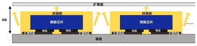
Package Structure Schematic
Doitvision Partner’s is a leading IDM (Integrated Device Manufacturer) of high-end semiconductor light sources. They have integration advantages across the industrial chain, with deep-rooted expertise in manufacturing, packaging, and testing processes.
To address the challenges in packaging path selection for Mini BLU (Backlight Unit), The Partner has iteratively innovated upon COB and traditional POB solutions, introducing its proprietary ACSP (Advanced Chip Scale Packaging) backlight technology. This breakthrough combines the strengths of both approaches while further enhancing performance and cost efficiency.
Performance Advantages
The Mini BLU adopts in-house flip-chip designs and the ACSP technology, achieving a compact package size of only 1.1-1.2 times the chip dimensions.
The light-emitting angle of the LEDs is extended from 140° to nearly 180°, enabling an ultra-thin 0OD (Zero Optical Distance) design for seamless color mixing.
This versatility supports applications across AR/VR, tablets/laptops, monitors, TVs, automotive displays, and other full-size display segments.
Additionally, the ACSP solution incorporates unique electrode expansion technology and secondary reflow soldering processes, effectively resolving yield issues caused by light leakage and uneven color mixing inherent to conventional CSP packaging.
Cost Optimization
Capitalizing on its vertically integrated supply chain, Our Partner implements end-to-end cost control spanning chip design, optical simulation, packaging processes, and driver design. The ACSP technology significantly improves production yields while further reducing manufacturing costs.
Conclusion
We have introduced the difference between COB and POB packaging technology. As a top COB LED display manufacturer, we always break new technology with our excellent partners. Therefore, our COB LED screen is not only of good quality, but also affordable. If you are interested in our COB LED display, please feel free to contact us.