 All-in-One COB LED TV
 Flexible LED Displays
 Transparent LED Displays
 Led Poster
 Circular LED Displays
 Creative & Custom LED Displays
LED packaging plays a pivotal role in determining the LED display performance, reliability, and longevity. The packaging process raw materials directly influence the electrical, thermal, optical, and mechanical characteristics of the final LED components. Do you know the key raw materials used in LED packaging? Today,Doitvision will guide you how each element contributes to building a high-quality LED solution.
LED Lead Frames
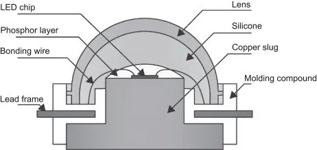
LED lead frames are the mechanical foundation and electrical interface for LED chips. Due to excellent electrical and thermal conductivity, they are primarily made of copper. However, other materials like iron, aluminum, and ceramics are also used for specific applications due to different thermal or structural properties.
The lead frame has internal conductive paths (leads) that establish electrical contact with the chip’s electrodes. Once the LED is fully packaged, the chip can be removed from the lead frame. Then, they are integrated into modules or LED display. The remaining “legs” or terminals are the positive and negative electrodes. So, it is easy to solder onto circuit boards or lighting fixtures.
Lead Frames Classification
Lead frames can be categorized based on different parameters:
By Product Type:
- SMD Lead Frames: Designed for surface mounting on PCBs.
- Through-Hole or DIP Frames: Used for through-hole soldering.
- Filament-Type Frames: Designed for LED filament bulbs.
- PCB Substrate: When used directly as the mounting and connection base.
By Material:
- Copper Frames: High conductivity and heat dissipation.
- Iron Frames: Cost-effective but less conductive.
- Aluminum and Ceramic Substrates: High thermal stability, often used in high-power or automotive LEDs.
- Bismaleimide Triazine Substrates: Used for high-frequency or high-reliability applications.
By Plating:
The lead frames surface finish affects solderability and corrosion resistance.
- Common finishes include:
- Copper-Nickel-Silver
- Nickel-Gold (electroplated or electroless)
- Soft Gold for wire bonding
- Nickel-Palladium-Gold
- chemical or OSP treatment
Plating thickness is often measured in microinches (uin or µin), where 1 µin ≈ 0.0254 µm.
LED Chips

The LED chip, also known as the light-emitting die, is the core semiconductor device responsible for light emission. It operates based on a P-N junction made from compound semiconductors. They are most commonly gallium-based materials, though silicon substrates may also be used in supporting structures.
When an electric current flows through the LED chip, electrons in the N-type region recombine with holes in the P-type region. This electron-hole recombination releases energy in the form of photon.
Key LED Chip Parameters
Each LED chip comes with a set of electrical and optical specifications:
- Type: Chip family or series
- Wavelength (WLD): Expressed in nanometers (nm)
- Luminous Intensity (LV): Measured in millicandelas (mcd) or milliwatts (mW)
- Forward Voltage (VF): Listed with minimum, typical (average), and maximum values
- Standard Deviation: Variability in brightness or color
Classification of LED Chips
By Color (Wavelength Range):
- Red (R): 620–760 nm
- Green (G): 492–577 nm
- Blue (B): 435–480 nm
By Chip Geometry:
- Round Chips (Wafer Form)
- Square Chips (Discrete Form)
By Structure:
- Vertical Structure: Single electrode at the bottom; better heat dissipation.
- Lateral or Horizontal Structure: Electrodes on the same plane; common for mid-power LEDs.
By Size (Mil):
- Red chips: typically 3.2 mil, 3.5 mil, 4.2 mil
- Blue/Green chips: 45 mil, 46 mil, 56 mil, up to 810 mil(Note: 1 mil ≈ 25.4 µm)
- The chip size and structure affects brightness, heat management, and overall reliability.
Die Attach Adhesive

Die attach adhesives secure the LED chip onto the lead frame and play a dual role: mechanical fixation and thermal/electrical conductivity.
There are two main types:
- Conductive Adhesive: They are often used in vertical structure LEDs (e.g., red LEDs). These adhesives contain silver or other conductive fillers to provide a low-resistance path for current.
- Insulating Adhesive: They are used with horizontal structure LEDs (e.g., blue and green LEDs).
Note:
Both electrodes are on top and require no conductive substrate.
Performance Requirements
High-quality die attach adhesives must offer:
- Strong adhesion and shear strength
- High thermal conductivity
- Low moisture absorption
- Chemical and UV stability
- Resistance to yellowing over time
Like Nationstar or Kinglight Top LED packaging manufacturers use premium-grade adhesives to ensure reliability and long service life.
Bonding Wire
Bonding wires, or interconnect wires, are ultra-fine conductors that connect the LED chip’s electrodes to the lead frame. They are used for electrical transmission and impact both performance and yield in LED packaging.
Related:
Gold Wire VS Copper Wire of LED Screen
Bonding Wires Types

By Material:
Gold (Au) Wire: Excellent conductivity and corrosion resistance but expensive.
- Silver (Ag) Wire: Good conductivity, lower cost than gold.
- Copper (Cu) Wire: Cost-effective, high strength, but easily oxidized.
- Palladium-Coated Copper (PCC) Wire: Combines conductivity and corrosion resistance.
- Aluminum (Al) Wire: Used in power electronics.
- Alloy Wire: For specific mechanical or thermal requirements.
By Diameter:
Common diameters include 0.7 mil, 0.8 mil, 0.9 mil, 1.0 mil(1 mil ≈ 25.4 µm)
The wire material and thickness affects bonding process parameters, electrical resistance, and thermal behavior.
Encapsulation Material
Encapsulation, or molding, protects the internal LED structure from external damage and enhances light extraction. It plays a vital role in waterproofing, dust resistance, and UV protection, while also contributing to light shaping and color stability.
Encapsulation Materials Types
Epoxy Resin
- Advantages: High light transmittance, strong adhesion, good mechanical properties, low cost
- Disadvantages: Poor UV resistance, prone to yellowing at high temperatures
Silicone Resin
- Advantages: Excellent transparency, UV resistance, and thermal stability; Good for outdoor or high-power LEDs
- Disadvantages: Lower adhesion to lead frames compared to epoxy
Modified Resin Systems
These hybrid materials are used to combine the benefits of epoxy and silicone:
- Physical Blends: Mixes of epoxy and silicone prepolymers with curing agents. While cost-effective, they suffer from compatibility issues and material separation.
- Chemical Modifications: Introduces epoxy groups into silicone molecules and enhance adhesion and mechanical strength.
- The encapsulant can improve LED lifespan, especially in outdoor or high-humidity applications.
Why Material Selection Matters
The LED package performance is only as strong as its weakest material. If the die attach has poor thermal conductivity, the chip may overheat. If the encapsulation yellows prematurely, brightness and color consistency will degrade. And if bonding wires are easily oxidized, long-term reliability suffers.
As an engineer, supplier, or manufacturer, your goal should always choose right materials for indoor signage, automotive lighting, or large-scale outdoor LED video walls.
Trends and Innovations in LED Packaging Materials
As LED technology advances, LED packaging materials continue to evolve. There are some several notable trends:
Miniaturization: With the rise of Mini LED and Micro LED, material tolerances are tighter and thermal efficiency becomes even more critical.
High Thermal Conductivity Materials: New ceramic and aluminum substrates are gaining traction to handle higher power densities.
Environmentally Friendly Encapsulants: Low-VOC and lead-free materials are now preferred, especially in Europe and North America.
Flip-Chip and COB Technology: These require advanced adhesives and encapsulants that can withstand high reflow temperatures and offer strong mechanical support.
Conclusion
We have guided you the raw materials behind LED packaging. As pfrofessional LED display manufacturers, we always choose high-quality components to build high quality LED display. If you have an LED display project, you can contact us.