As small-pitch COB LED screens become more and more popular, do you know how this innovative packaging technology revolutionizes the integration of electronic components? Why can this technology create smaller and more efficient devices? Today Doitvision will introduce you to the COB technology details.
What is a Chip-on-Board (COB) PCB?
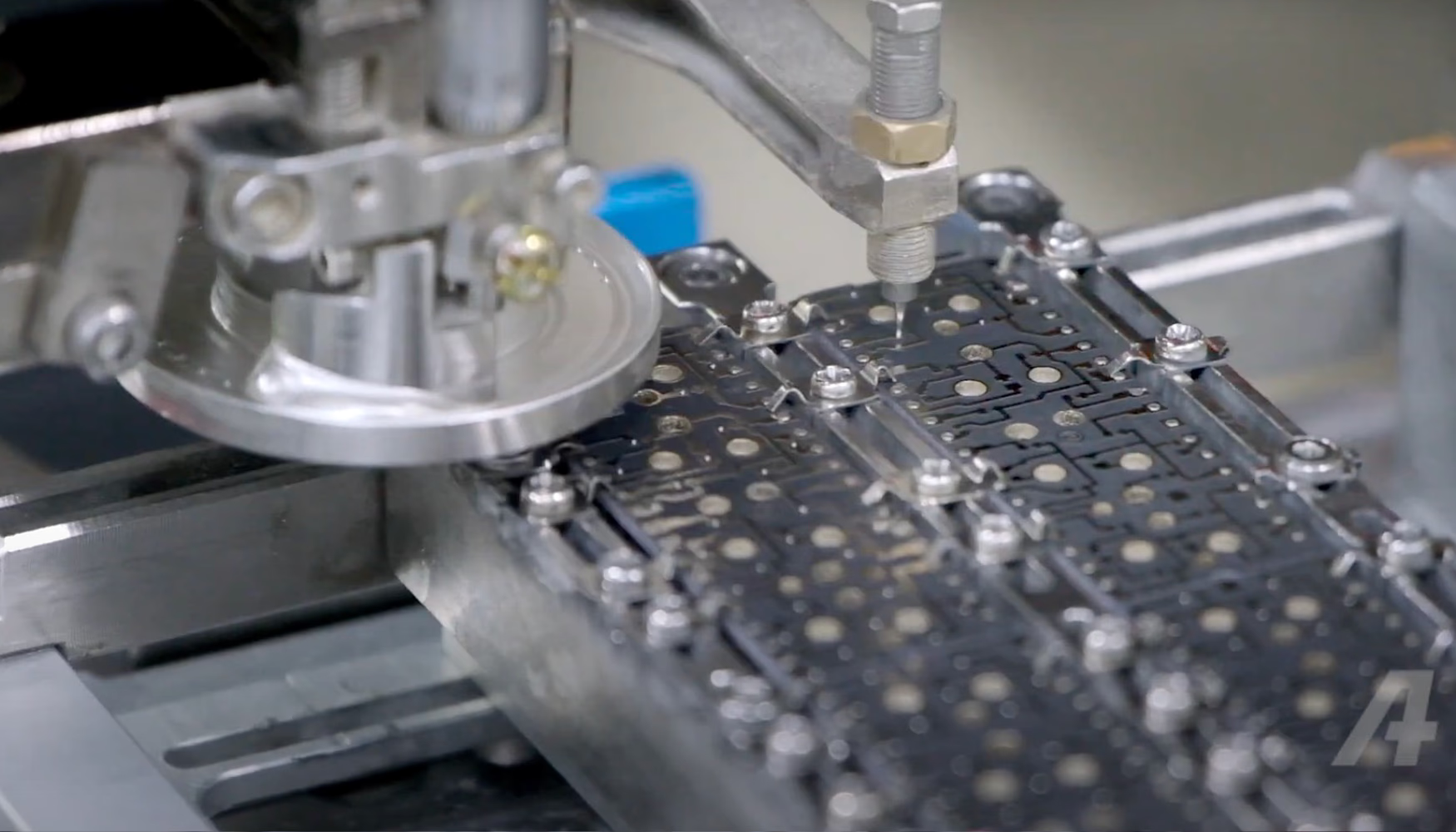
COBtechnology is a method of directly mounting electronic components onto a PCB. In this approach, bare integrated circuits (ICs) are attached to the PCB surface without using traditional standalone packaged components. So, it can eliminate reliance on conventional ceramic or plastic packaging, enabling smaller and lighter electronic devices and systems.
For chip installation, solder bumps or adhesives are employed to achieve a compact and efficient assembly. The direct bonding creates shorter electrical pathways between the chip and the PCB, delivering superior electrical performance and minimizing signal loss.
Additionally, COB technology offers effective thermal management, as the chip makes direct contact with heat sinks or thermal pads integrated into the board.
Due to excellent electrical performance, compact footprint, and robust thermal properties,COB is ideal for space-constrained applications,such as:
- wearable devices
- mobile phones
- LED lighting
- power electronics.
Furthermore, COB technology drives advancements in miniaturization and enables highly integrated electronic systems.
How Are COB PCBs Manufactured?
Substrate Preparation:
The process begins by cleaning the PCB surface and applying a conductive adhesive to predefined areas where chips will be bonded.
Die Attachment:
Bare dies (unpackaged semiconductor chips) are picked up and precisely placed onto the adhesive-coated PCB regions. It typically use pick-and-place machines or specialized equipment.
Bonding:
Once positioned, the chips are bonded to the board using conductive solder bumps. This creates reliable electrical connections between the die and the PCB’s conductive traces.
Wire Bonding:
In some cases, wire bonding is employed, where thin metal wires (often gold) connect the chip’s contact pads to the PCB traces to transmit electrical signals.
Encapsulation:
Encapsulation material, such as epoxy resin, is applied to protect the chips and bonding wires from environmental factors. This forms a protective layer over the assembly.
Testing:
The COB assembly undergoes rigorous testing, including thermal cycling, electrical performance checks, and visual inspections, to ensure reliability and functionality.
Final Assembly:
After passing all tests, the COB PCB is ready for integration into end-use devices like LED fixtures, smartphones, or other electronics.
Key Technical Insights:
COB technology bonds semiconductor dies directly to the PCB substrate using adhesives, then connects them to the board’s circuitry and encapsulates the assembly. It optimizes SMT by eliminating the need for traditional component packaging.
COB vs. SMT:
The fundamental difference lies in COB’s focus on high-pin-count active components (e.g., ICs) without requiring ceramic or plastic packaging. So, it enables thinner, lighter, and more densely integrated designs compared to conventional SMT approaches.
Dialysis Chip on Board Application
.JPEG)
COB technology involves directly mounting bare semiconductor dies onto a printed circuit board (PCB). After wire connections are completed, an epoxy resin encapsulation is typically applied over the chip to protect the interconnects. The bare die is secured to the PCB using adhesives and electrically connected to the board’s conductive traces via wire bonding. Finally, epoxy resin provides insulation and protection.
In this process, unpackaged integrated circuits (ICs) are mounted on a PCB, which may include signal conditioning and support circuitry. Electrical connections between the IC and corresponding PCB pads are established using gold wire bonding. A protective coating is then applied over the chip to safeguard it and its bonding wires.
Key Advantages of COB Technology:
Miniaturization: COB is an ideal solution for reducing circuit size and weight, particularly when traditional assembly methods fail to meet design constraints.
Compact Design: By eliminating bulky component packaging, COB significantly reduces the system’s footprint, making it ideal for miniaturization applications.
Assembly Flexibility: COB offers unique integration options. Silicon dies are directly adhered to the PCB surface and connected via conductive pads or gold wires. An opaque epoxy protective layer is added to shield the assembly from mechanical stress and harmful light exposure.
Technical Workflow:
- Die Attachment: The bare die is bonded to the PCB using adhesives.
- Wire Bonding: Gold wires create electrical pathways between the die and PCB traces.
- Encapsulation: Epoxy resin is applied to insulate and protect the assembly.
- Protective Coating: A final layer ensures durability against environmental factors.
COB technology enables highly compact, lightweight, and reliable systems, making it particularly valuable in medical devices like dialysis equipment, where precision, durability, and space efficiency are paramount.
Key Features and Advantages of COB Technology
- High- & Low-Voltage Design: Supports both high- and low-voltage applications for versatile use cases.
- Custom Coatings: Tailored encapsulation materials (e.g., epoxy, silicone) enhance durability and environmental resistance.
- Multilayer & Double-Sided PCBs: Enables complex circuitry and high-density integration.
- Functional Board Testing: Rigorous pre- and post-assembly testing ensures reliability and performance.
- High- or Low-Volume Production: Scalable for mass production or niche, low-volume applications.
- Wide Temperature Range: Operates reliably in extreme temperatures (-40°C to +150°C).
- Cost-Competitive Solutions: Reduces material and assembly costs by eliminating traditional packaging.
- Turnkey Solutions: End-to-end design, assembly, and testing services streamline development.
Total Cost of Ownership: COB LED vs SMD LED
When evaluating a COB LED display investment, the true measure is the total cost of ownership over a typical 5-year lifecycle. COB technology shifts spending from ongoing corrective maintenance to an initial quality investment.
Initial Acquisition Cost For fine-pitch displays below P1.5, COB panels can carry a 10-20% premium over equivalent SMD modules. This is due to the precise die-attach and encapsulation processes. However, this gap is narrowing as flip-chip COB manufacturing scales.
The Hidden Savings: Maintenance and Labor This is where COB fundamentally changes the budget. SMD lamps are exposed; a single errant touch, cleaning accident, or shipment vibration can knock off individual LEDs. The result is on-site repair labor, specialist technicians, and rental lifts . The costs often surpass the module price within two years. COB’s hard epoxy layer completely encases the LED dies. The surface is anti-scratch and impact-resistant. Doitvision’s COB panels exhibit a dead-pixel rate below 5 PPM at delivery, and this near-perfect state remains stable for years. For a 50-square-meter control room video wall, you can choose COB LED screen. It can eliminate 5,000−15,000 in post-installation repair labor over the screen’s life.
Energy Consumption Flip-chip COB designs deliver more lumens per watt. By removing the wire-bond obstruction and improving thermal pathways, the drive current can be reduced for the same perceived brightness. In a 24/7 operational scenario, a large COB display can reduce electricity costs by approximately 15-20% . This ongoing saving directly impacts facility operating budgets.
A Practical Cost Scenario: 5-Year Projection for a 20 sqm P1.2 Video Wall
| Cost Factor | Typical SMD Solution | Doitvision COB Solution |
|---|---|---|
| Initial hardware & installation | $200,000 | $225,000 |
| On-site repair labor (est.) | $12,000 | $800 |
| Replacement modules/parts | $3,000 | $500 |
| 5-year energy cost difference | $18,000 | $14,400 (20% less) |
| Total 5-Year Cost | $233,000 | $240,700 |
| Year 6+ Annual Cost | Higher maintenance & energy | Lower maintenance & energy |
While the initial investment for COB is slightly higher, the drastic reduction in unplanned maintenance, coupled with energy savings, So, the total cost of ownership equalizes within the warranty period. It becomes significantly lower thereafter. More importantly, you avoid the operational risk of screen downtime in a critical environment.
COB vs SMD vs GOB vs DIP: Which LED Technology Wins Below P1.5?
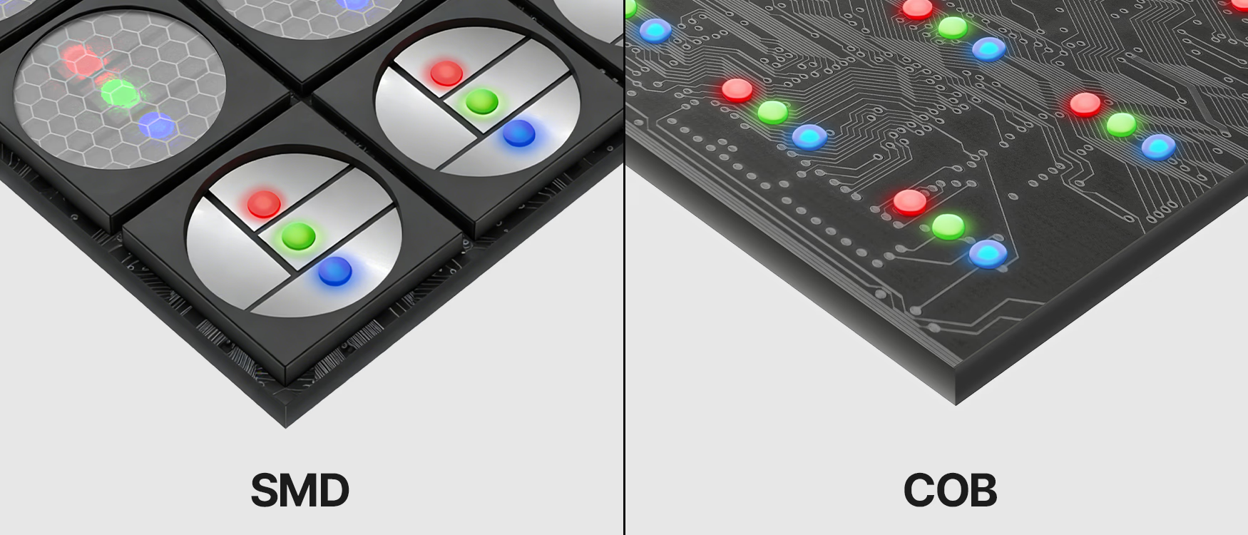
Below, we objectively evaluate the four mainstream technologies to help you make a data-driven decision.
| Performance Parameter | COB (Chip on Board) | SMD (Surface Mounted) | GOB (Glue on Board) | DIP (Dual In-line) |
|---|---|---|---|---|
| Minimum Pitch | P0.4mm+ | P0.9mm+ | P1.2mm+ | P4mm+ |
| Protection Level | Excellent (encapsulated face) | Poor (exposed lamps) | Good (glue layer) | Good (lens sealed) |
| Impact Resistance | Very High (>IK08) | Low (lamps knock off) | Medium-High | High |
| Dead Pixel Rate | <5 PPM (inherently stable) | Higher after transport/use | Reduced vs SMD | Low |
| Surface Flatness & Blackness | Superior matte black, no reflection | Lamp bead relief, visible gloss | Glue layer may show unevenness | Large pixel gaps |
| Heat Dissipation | Direct die-to-PCB path, excellent | Through lamp leads, fair | Glue traps some heat | Through leads, fair |
| Viewing Comfort | Very high (no moiré, no glare) | Prone to moiré and graininess | Improved over SMD | Low (outdoor use) |
| Repairability | Module-level replacement recommended | Individual lamp can be reworked | Individual lamp repair difficult | Lamp can be replaced |
| Relative Cost (P1.2) | Moderate-High | Moderate | Moderate-Low | N/A for fine pitch |
Sub-P1.5mm Applications
- SMD remains cost-competitive for P1.8 and above, where pixel pitch is larger and damage risk is lower.
- GOB is an add-on process that improves SMD robustness, but it does not address the underlying pixel-level blackness and thermal limitations inherent to discrete lamp beads.
- COB is the superior architectural choice for seamless viewing application at close range, zero-distraction reliability, and long-term stability. This is why Doitvision focuses our engineering team exclusively on advancing flip-chip COB for control rooms, studios, and high-end corporate spaces.
What Are COB LED Lights?
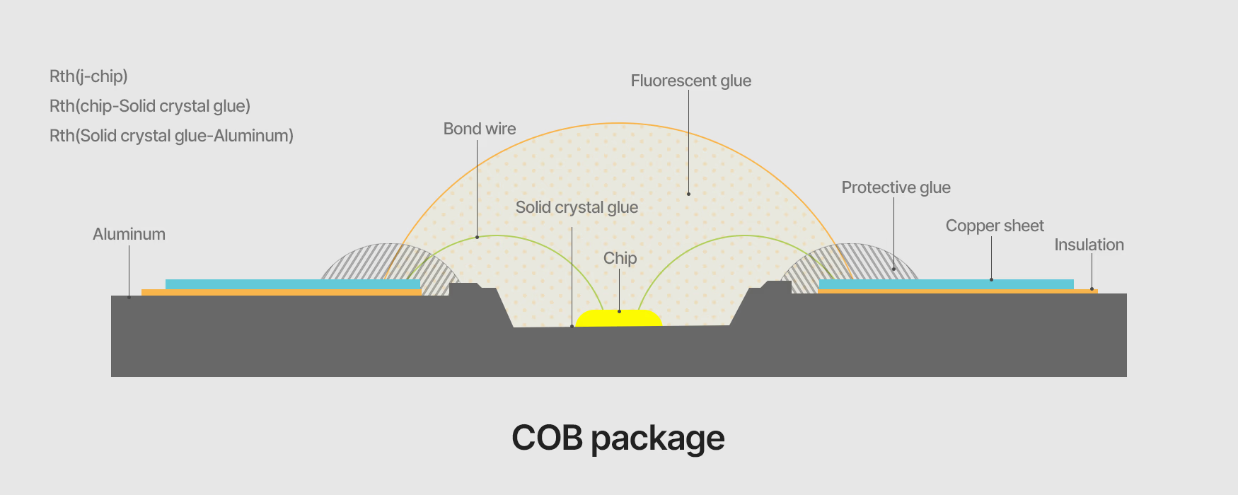
COB LED technology involves mounting multiple LED chips directly onto a substrate material (e.g., silicon carbide SiC or sapphire) to create a densely packed LED array. As a newer and technologically advanced approach, COB LEDs offer significant advantages over traditional LED designs:
Higher Lumen Density: Achieved by integrating multiple LED chips into a single array, unlike older technologies that rely on single DIP LEDs or a few SMD LEDs.
Uniform Light Output: Closely spaced chips produce consistent, high-intensity illumination with minimal shadowing or hotspots.
Space Efficiency: Compact design reduces the footprint while maintaining high brightness.
Simplified Circuitry: Most COB designs use a single-circuit configuration with two contacts, streamlining assembly and electrical connections.
Key Benefits of COB LED Technology:
- Ultra-Compact Size: It is Ideal for space-constrained applications.
- Enhanced Brightness: Delivers superior intensity, especially at close range.
- Uniform Illumination: Consistent light distribution for precision tasks.
- Streamlined Design: Simplified thermal and electrical management.
- Improved Thermal Performance: Direct substrate bonding enhances heat dissipation, boosting reliability and lifespan.
COB LEDs are widely used in automotive lighting, medical devices, stage lighting, and consumer electronics.
Advanced COB Architecture: Wire-Bonding vs. Flip-Chip
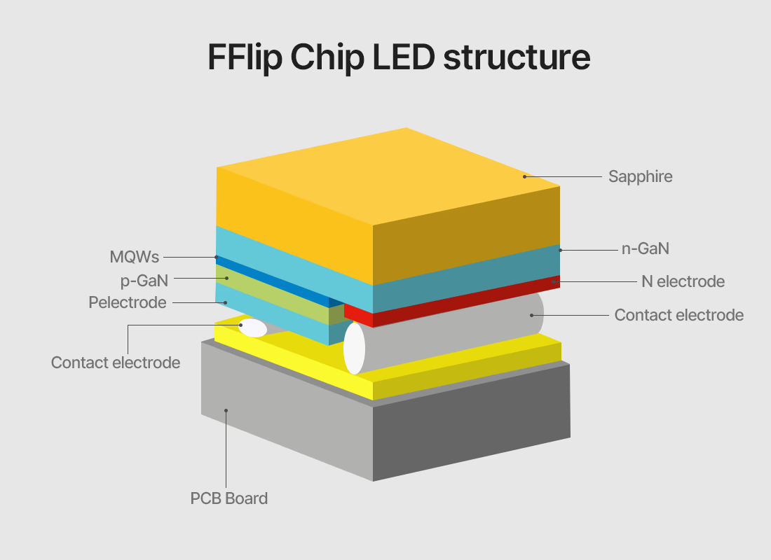
Not all COB LED displays are created equal. The fundamental differentiator lies in how the LED chip is connected to the substrate. As a professional buyer, you need long-term reliability and visual performance.
Wire-Bonding COB (Traditional Approach) In this architecture, the bare LED chip is mounted face-up. Extremely thin gold wires are used to connect the chip’s top electrodes to the PCB pads, before the whole assembly is encapsulated. While cost-effective and mature, this design introduces two potential weaknesses: the delicate gold wires remain a point of failure, especially under thermal expansion stress, and the wires partially obstruct light emission, causing minor shadows and uneven luminance at extreme angles.
Flip-Chip COB (Next-Generation Standard) This is the technology that truly unlocks the potential of ultra-fine pitch LED displays. The LED chip is inverted and bonded directly to the substrate via metal bumps or pillars. It eliminates the need for any gold wire.
- Superior Thermal Management: The heat generated at the light-emitting layer is conducted directly into the PCB through the shortest possible path, without passing through a poorly conductive sapphire substrate. Compared to wire-bonding,this reduces the thermal resistance by up to 5 times. So, it dramatically extends the LED’s lifespan, reducing brightness degradation.
- Unobstructed Light Output: With no wires on the emitting surface, flip-chip COB delivers a wider, more uniform light field. It completely eliminates the risk of “caterpillar” dead pixel clusters caused by wire breakage.
- Enhanced Reliability: The all-metal, solid-state bonding is inherently more robust against physical shock and thermal cycling. Therefore, flip-chip COB screens are ideal for rental staging, luxury retail, and mission-critical control rooms.
At Doitvision, our current mass-production priority is flip-chip COB LED screen. You can supply your clients with the most stable, visually stunning technology available today.
Common Cathode COB LED Technology
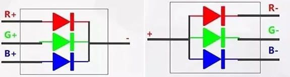
Common cathode technology is an energy-saving power supply design. It is widely adopted in high-end COB LED displays.
Traditional LED displays often use a common anode structure, where different LED chips share the same voltage supply. In contrast, common cathode technology supplies separate voltages to red, green, and blue chips independently.
This optimized power distribution reduces unnecessary energy loss and heat generation.
Advantages of common cathode COB LED displays include:
· 20%–40% lower power consumption
· Reduced operating temperature
· Improved display stability
· Longer LED lifespan
· Better energy efficiency
For applications requiring 24/7 operation, such as control rooms and monitoring centers, Doitvision's common cathode COB displays provide significant long-term operational savings.
COB LED Display Contrast Ratio and HDR Performance
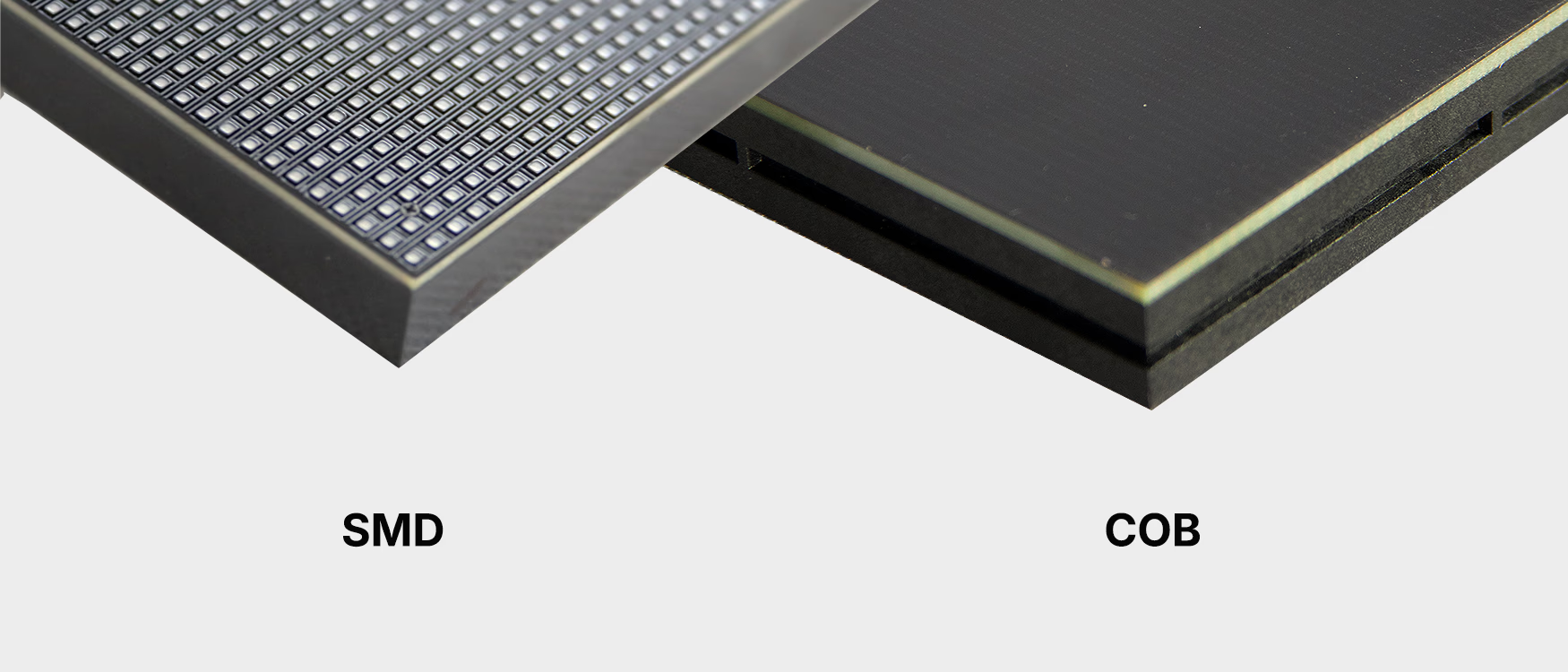
One of the biggest advantages of COB LED displays is their outstanding image quality.
Because COB technology creates an ultra-flat display surface with minimal light reflection. Compared with traditional SMD LED display, it achieves significantly better black levels and contrast performance s.
Modern COB LED displays can achieve contrast ratios exceeding 10,000:1, delivering:
· Deeper black performance
· Better grayscale transition
· Improved HDR effect
· Higher image depth
· Enhanced visual realism
| Technology | Typical Contrast Ratio |
|---|---|
| Traditional SMD LED | 4,000:1 – 6,000:1 |
| COB LED Display | 10,000:1 – 20,000:1 |
Many premium COB LED displays also support HDR10 technology:
· XR virtual production
· Broadcast studios
· Corporate showrooms
· High-end conference rooms
· Luxury retail applications
Recommended Viewing Distance for COB LED Displays
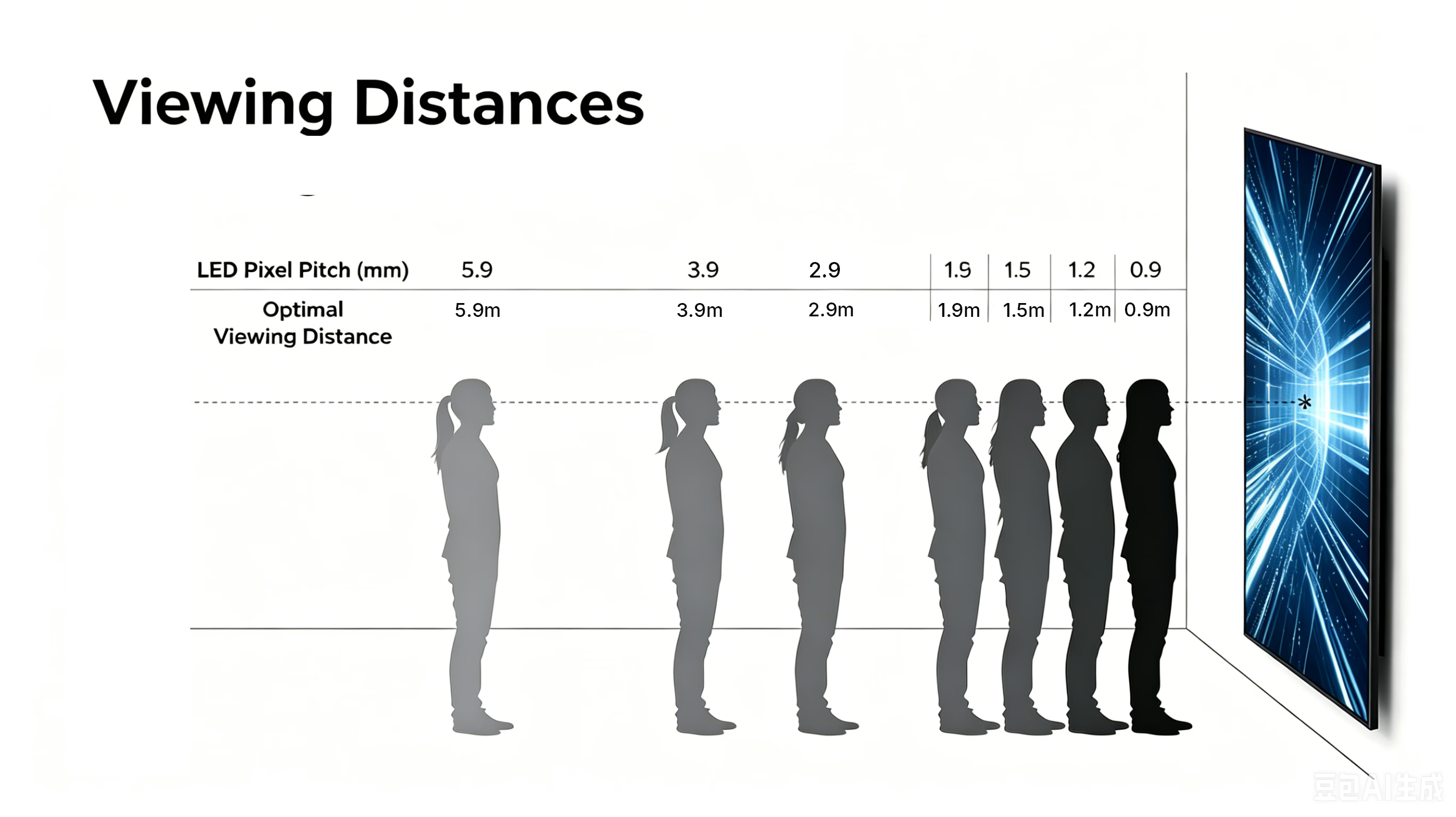
Generally, the minimum viewing distance is approximately equal to the pixel pitch value in meters.
| Pixel Pitch | Recommended Minimum Viewing Distance |
|---|---|
| P0.7 COB | 0.7m |
| P0.9 COB | 0.9m |
| P1.2 COB | 1.2m |
| P1.5 COB | 1.5m |
| P1.8 COB | 1.8m |
For close-viewing indoor environments such as meeting rooms and studios, smaller pixel pitch COB displays provide superior image clarity and smoother visual performance.
4K COB LED Display Size Calculator

Many customers want to know what screen size is required to achieve true 4K resolution using COB LED displays.
The required display size depends on the pixel pitch selected.
| Pixel Pitch | Approximate 4K Screen Size |
|---|---|
| P0.9 COB | 110 inches |
| P1.2 COB | 146 inches |
| P1.5 COB | 183 inches |
| P1.8 COB | 220 inches |
For premium meeting rooms and broadcast environments, P1.2 COB is one of the most popular choices because it offers an excellent balance between image quality and project cost.
COB Packaging Process

COB technology offers cost-effective, space-saving solutions. It has a mature manufacturing process compared to other packaging methods. However, it also presents specific limitations and technical challenges.
Advantages:
- Lower Cost: COB packaging is approximately one-third the price of equivalent traditional packaging.
- Space Efficiency: Eliminates bulky component casings, enabling compact designs.
- Proven Manufacturing: Leverages established processes for reliable production.
Limitations:
- Equipment Requirements: It requires specialized soldering and encapsulation tools, potentially slowing production rates.
- Environmental Sensitivity: Strict control over humidity, temperature, and cleanliness is critical during PCB assembly.
- Maintenance Complexity: Repairs or rework are challenging due to the integrated, encapsulated design.
Performance Considerations:
Enhanced Signal Integrity: By minimizing parasitic effects from packaging materials, COB can improve IC performance.
Design Challenges:
Substrate Connectivity: Lead-frame chips or BGA (Ball Grid Array) configurations in COB designs may lead to suboptimal VCC/ground connections.
CTE Mismatch: Differences in the coefficient of thermal expansion (CTE) between materials can induce mechanical stress, risking solder joint or trace failures.
Thermal Management: Requires careful design to mitigate heat buildup in densely packed layouts.
COB remains a popular choice for applications prioritizing cost and miniaturization, but its technical constraints necessitate careful design and process optimization.
Step 1: Crystal Expansion
The expansion machine uniformly stretches the manufacturer-provided LED chip film. It separating tightly arranged LED chips attached to the film surface to facilitate pick-and-place operations.
Step 2: Adhesive Application
Place the expanded crystal ring on a backing machine surface coated with silver paste. A dispensing machine applies an appropriate amount of silver paste to the PCB for batch LED chip mounting.
Step 3: LED Chip Placement on PCB
Load the silver paste-coated expanded crystal ring into a pick-and-place machine. Operators use a bonding tool under microscopy to precisely position LED chips on the PCB.
Step 4: Thermal Cycling of Perforated PCB
Place the perforated PCB in a thermal cycle oven for controlled dwell time. Remove once the silver paste cures (prolonged exposure may oxidize/yellow LED coatings). This step applies only to LED chip bonding, not IC chip bonding.
Step 5: IC Chip Attachment
Apply red adhesive to IC positions on the PCB using a dispenser. Position IC dies accurately on the adhesive using anti-static tools (red or black adhesive variants).
Step 6: Curing Process
Place adhesive-bonded components in a thermal cycle oven on a large flat heating plate for temperature-stable curing. Natural curing is optional but requires extended time.
Step 7: Wire Bonding
Use an aluminum wire bonder to create interconnections between chip pads (LED/IC) and corresponding PCB pads, completing COB (Chip-on-Board) internal wiring.
Step 8: Pre-Testing
Evaluate COB boards using specialized test equipment (e.g., high-precision stabilized power supplies). Reject and rework non-compliant units.
Step 9: Encapsulation
Apply measured AB epoxy to bonded LED modules using a dispenser. Encapsulate ICs with black epoxy, followed by cosmetic encapsulation per customer specifications.
Step 10: Final Curing
Cure encapsulated PCBs in a thermal cycle oven under controlled temperature. Adjust drying times per process requirements.
Step 11: Post-Testing
Perform electrical performance testing on encapsulated PCBs using dedicated test tools to finalize quality grading.
COB LED Display Price Guide
COB LED display price depends on multiple factors, including pixel pitch, brightness, cabinet materials, refresh rate, and system configuration.
Below is a general reference price range for indoor COB LED displays.
| Pixel Pitch | Typical Application | Estimated Price Range |
|---|---|---|
| P0.7 COB | XR Studio / Broadcast | $6,000–$9,000/sqm |
| P0.9 COB | Control Room | $4,000–$5,000/sqm |
| P1.2 COB | Meeting Room | $2,500–$4,500/sqm |
| P1.5 COB | Retail Display | $1,800–$3,000/sqm |
Conclusion:
COB technology has dramatically changed the electronics industry. It provides more advantages not available with traditional packaging technologies.
With chips mounted directly on the board, COB technology enables electronic devices to be smaller, lighter, and more energy efficient. Due to removing excess packaging and shortening electrical connection paths,so it improves electrical performance, reduces signal loss, and facilitates effective thermal management. Through this cutting-edge technology, it makes COB displays become more and more HD. As a top COB LED vvideo wall manufacturer, if you need COB LED displays, please feel free to contact us.
Breaking the boundaries of the flat screen allows for unprecedented spatial experiences. Whether it's a gaming kiosk or a massive architectural pillar, if you have an unconventional idea, don't let standard hardware specifications limit you. The engineering exists to build it.

The Author
Kris Liang
Founder & Lead Engineer, DOIT VISION
With nearly two decades of experience bridging Shenzhen's manufacturing capabilities with Western architectural needs, Kris specializes in translating complex visual concepts into reliable, deployable hardware. He is passionate about structural engineering and high-reliability AV solutions.
kris@doitvision.com