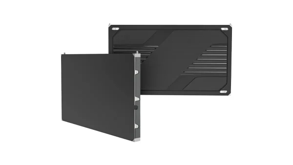
All-in-One COB LED TV
 Flexible LED Displays
 Transparent LED Displays
 Led Poster
 Circular LED Displays
 Column LED Screens
 Creative & Custom LED Displays
COB flip-chip technology — the engineering foundation behind every All-in-One LED TV. Sealed wipe-clean surface, scratch-resistant epoxy, 7,000:1 contrast, how it compares to SMD, why fewer than 10 factories worldwide produce it at scale, and whether it’s the right choice for your meeting room.
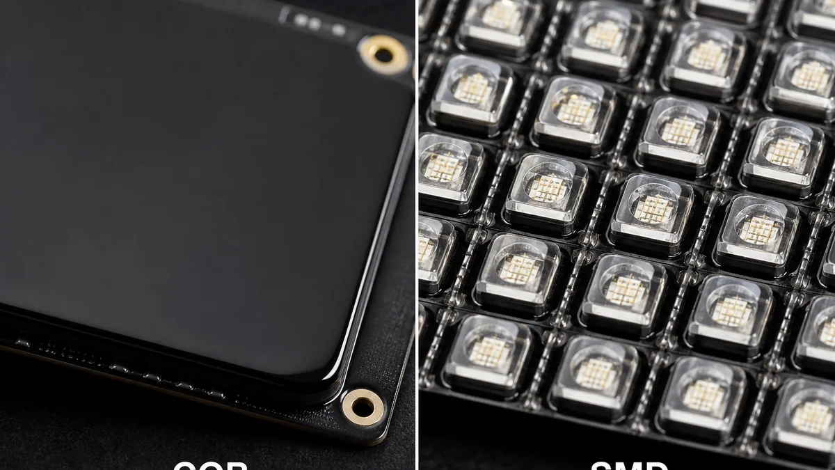
- COB (Chip on Board) bonds LED chips directly to the PCB and encapsulates the entire surface in epoxy — eliminating individual LED packages, bond wires, and the gaps between pixels that SMD displays exhibit.
- Five engineering advantages: a sealed surface (wipe clean with a damp cloth), scratch-resistant epoxy, 7,000:1 native contrast (deep blacks in bright rooms), 160° viewing angle, and fewer dead pixels over lifetime due to flip-chip design.
- For fine-pitch displays (P0.93–P1.56) above 100 inches, COB is price-competitive with equivalent SMD when you factor in the reduced failure rate and zero maintenance costs over a 5-year lifecycle.
- COB manufacturing requires a cleanroom environment and micron-level PCB flatness. Fewer than 10 factories worldwide produce COB LED at scale for displays above 100 inches. DOIT VISION is one of them.
What COB LED Technology Actually Is
COB stands for Chip on Board. It is a method of LED packaging where the red, green, and blue LED chips are bonded directly to the PCB substrate — without any individual plastic housing around each pixel. The entire surface is then encapsulated in epoxy resin as one continuous layer, creating a seamless, glass-like display surface.
This is fundamentally different from traditional SMD (Surface Mount Device) technology, where each RGB LED sits inside its own tiny plastic package with bond wires connecting the chip to the package pins, and those pins are then soldered to the PCB. On an SMD display, every pixel is a physically separate component — with air gaps between them.
The Flip-Chip Variant: Engineering That Eliminates the Weakest Link
Within COB technology, the flip-chip variant takes reliability one step further. Instead of an LED chip sitting upright with bond wires connecting its top surface to the PCB, the chip is mounted upside down — its electrical contacts face the PCB directly. No bond wires are needed.
Why does this matter? Bond wires are statistically the most failure-prone component in LED displays. They are thinner than a human hair, subject to thermal expansion stress during daily on/off cycles, and vulnerable to vibration during shipping and installation. Eliminating them removes the single biggest source of dead pixels over the display’s lifetime.
SMD puts each pixel in its own tiny plastic house with fragile bond wires inside. COB eliminates the houses entirely — every pixel lives directly on the PCB under one continuous protective roof.
The Five Engineering Advantages of COB LED
Each of these five advantages is a direct consequence of the chip-on-board architecture. They are not marketing claims — they are physical properties of the design.
1. Sealed, Wipe-Clean Surface
The continuous epoxy layer seals the entire screen surface. There are no gaps, no exposed diodes, no openings for dust or moisture to enter. Coffee spills, fingerprints, and cleaning fluid wipe off with a damp cloth. This is a sealed surface, not a perforated one.
2. Scratch-Resistant Epoxy Surface
The epoxy encapsulation layer resists scratches from keys, pens, jewelry, and cleaning equipment. In a meeting room environment where people gesture near the screen, lean presentation clickers against it, or brush past it during room changes — this matters more than you’d think. An SMD screen struck by a key will lose that pixel permanently.
3. 7,000:1 Native Contrast Ratio
Between pixels on a COB display, the space is filled with black epoxy resin. This resin absorbs ambient light rather than reflecting it. The result: in a bright meeting room with floor-to-ceiling windows, a COB screen’s blacks remain black. An equivalent SMD screen shows dark gray — because the white plastic substrate between its individual LED packages reflects light back at the viewer.
4. 160° Viewing Angle with No Color Shift
The uniform epoxy surface eliminates the parallax and angular color shift that SMD panels produce at extreme angles. When someone sits at the far end of a wide conference table — 45° or more off-axis — a COB display shows the same color and brightness as it does head-on. On SMD, the individual LED packages cast tiny shadows on each other at angle, producing visible color drift.
5. Fewer Dead Pixels Over Lifetime
Flip-chip COB eliminates bond wires — the most common failure point in SMD LEDs. An SMD LED package contains up to 6 bond wires per pixel (2 per chip for RGB). Over thousands of thermal cycles, bond wires crack or detach. A COB flip-chip pixel has zero bond wires. The failure rate over a 50,000-hour operating life is measurably lower.
| Advantage | Engineering Root Cause | Real-World Impact |
|---|---|---|
| Sealed Surface | Continuous epoxy layer, no gaps | Dust-proof, wipe-clean with damp cloth |
| Epoxy Hardness | Hardened epoxy encapsulation | Resists keys, pens, accidental contact |
| 7,000:1 Contrast | Black epoxy between pixels absorbs light | True blacks in bright rooms |
| 160° Viewing | Uniform planar surface, no pixel-level shadows | No color shift at wide angles |
| Fewer Dead Pixels | Flip-chip: zero bond wires per pixel | Lower failure rate over 50,000h |
COB vs SMD: A Visual and Technical Comparison
If you place a COB panel and an SMD panel side by side in a brightly lit room, the differences are visible immediately — even to someone who has never seen an LED display before. Here is what you will see, and the engineering behind it.
| Factor | COB LED | SMD LED |
|---|---|---|
| Contrast Ratio | 7,000:1 — deep blacks in bright rooms | 5,000:1 — dark gray when ambient light is present |
| Surface Protection | Sealed epoxy, wipe-clean | Exposed LED diodes with gaps where dust accumulates |
| Pixel Structure | Smooth continuous surface, no visible pixel grid | Individual dots with visible gaps between pixels |
| Heat Dissipation | Direct PCB bonding — efficient thermal path | Package-to-board — thermal resistance at the solder joint |
| Best Pitch Range | P0.93–P1.56 | P1.5+ |
A 7,000:1 contrast ratio means COB produces noticeably deeper blacks than SMD at 5,000:1. In a meeting room with daylight streaming through windows, the difference between “black” and “gray background” determines whether text, spreadsheets, and presentation slides remain readable or wash out. This is the single most visible advantage of COB in real-world conditions.
Why COB Matters Specifically for Meeting Rooms
Meeting rooms place four specific demands on a large-format display — and COB addresses all four because of how it is built, not because of any added feature.
- Ambient light from windows and overhead lighting. Most meeting rooms have floor-to-ceiling windows or bright recessed lighting — the exact conditions where a 5,000:1 contrast ratio falls apart. COB delivers 500 nits brightness combined with 7,000:1 contrast, keeping presentation slides, spreadsheets, and video calls crisp and readable. SMD at 5,000:1 contrast produces a visible gray wash over everything.
- People touching the screen during presentations. Presenters gesture toward charts. Colleagues walk up to point at data. Someone leans a pen against the surface. An SMD screen accumulates dead pixels from these accidental contacts. COB’s sealed epoxy surface is impervious to them.
- Coffee cups on the conference table near the display. Spills happen. On SMD, liquid seeps into the gaps between LED packages and corrodes internal contacts. On COB, a spill sits on the sealed epoxy surface and wipes away with no damage.
- Long daily run times — 8 to 12 hours of continuous operation. Meeting room displays run all day, every workday. Bond wires in SMD LEDs expand and contract with each thermal cycle. Over years, this fatigue produces dead pixels. COB flip-chip has no bond wires to fatigue.
The combination of these four factors means that for a corporate meeting room with ambient light, the choice between COB and SMD is not about picture quality preferences — it is about whether the display will still look good in year three.
Tell us your room dimensions, ambient light conditions, and viewing distance. We’ll confirm whether COB is the right choice — or if SMD meets your needs at a lower cost.
The Manufacturing Difference: Why COB Is Hard to Make
COB manufacturing is fundamentally different from SMD assembly. SMD uses standard pick-and-place machines — the same equipment that builds smartphone circuit boards and laptop motherboards. Hundreds of factories own this equipment. COB requires three things that most LED factories do not have.
1. Cleanroom Environment
A single dust particle trapped between the LED chip and the epoxy encapsulation layer creates a visible defect on the finished display. Unlike SMD, where an individual LED package can be reworked, a COB defect in the encapsulation layer affects an entire module. Manufacturing must happen in a controlled cleanroom with filtered air, static control, and operator gowning — the same class of facility used for semiconductor fabrication.

2. Micron-Level PCB Flatness
The PCB substrate must be perfectly flat within microns across the entire panel surface. If the substrate is uneven, the epoxy layer thickness varies — creating optical distortion, brightness inconsistency, and visible banding. Standard PCB manufacturing tolerances (±0.2mm) are not good enough. COB-grade PCBs require specialized substrate materials and precision lamination processes.
3. Uniform Epoxy Application
The epoxy resin must be applied at a perfectly uniform thickness across the entire display surface. Variations thinner than a human hair create visible color shifts and brightness hot spots. The application process is proprietary to each manufacturer — the specific resin formula, curing temperature profile, and application method are closely guarded trade secrets that took years of iteration to perfect.
Fewer Than 10 Factories Worldwide
The combination of cleanroom infrastructure, precision PCB fabrication, and proprietary epoxy processes means that fewer than 10 factories worldwide produce COB LED at scale for displays above 100 inches. DOIT VISION manufactures COB modules at our Shenzhen facility — one of the few factories globally that controls the full COB production chain from PCB to finished module.
DOIT VISION operates an in-house COB production line in Shenzhen. We do not outsource COB module manufacturing to third parties. Customers receive factory inspection reports, aging test data, and pre-shipment photos of their specific units — including COB surface uniformity measurements under standardized lighting conditions.
Common Myths About COB LED — Debunked
COB technology has been commercially available for less than a decade, and three persistent myths circulate among buyers who heard about COB from competitors selling SMD. Here are the facts.
Myth 1: “COB panels can’t be repaired — if a pixel fails, you replace the whole screen.”
False. Individual COB LED modules are designed to be replaced at the module level — not repaired at the chip level. If a module develops a fault, a local technician swaps it in under 15 minutes. No realignment of adjacent panels is needed because the module-to-module mechanical tolerances are built into the frame. Replacement modules are dispatched within 48 hours during the 2-year warranty period. The process is faster than SMD rework, which often requires soldering individual LED packages on-site — a job few AV integrators want to perform.
Myth 2: “COB costs 2× the price of SMD.”
False — at scale, for the right pitch range. For P0.93 to P1.56 pixel pitches in displays above 100 inches, COB pricing is competitive with equivalent SMD when you factor in the reduced failure rate and zero maintenance costs over a 5-year lifecycle. SMD remains more cost-effective at coarser pitches (P1.8 and above), where the manufacturing precision advantage of COB is less relevant and SMD’s simpler assembly dominates on unit cost.
Myth 3: “COB has worse color uniformity than SMD.”
False. The continuous epoxy layer actually improves color uniformity by eliminating the individual-package color variations that SMD panels exhibit. In SMD manufacturing, each LED package comes from a different binning batch — and even within the same batch, slight color temperature variations between individual packages are visible when you look at a white field. COB’s uniform epoxy layer optically blends pixel-to-pixel variations, producing a visibly more consistent image — especially on solid-color backgrounds common in corporate presentations.
Is COB Right for Your Project? A Decision Checklist
COB is not always the right answer. The following checklist walks you through the five factors that determine whether COB LED is worth the investment — or whether SMD is the more sensible choice.
| If your answer is YES… | Your best choice |
|---|---|
| Your display will be in a room with ambient light? | COB — 7,000:1 contrast keeps blacks black |
| Viewers will sit closer than 2 meters? | COB — smooth surface, no visible pixel grid |
| The screen might be touched or bumped? | COB — sealed epoxy surface |
| You want the lowest maintenance over 5 years? | COB — fewer dead pixels, zero consumables |
| Your budget is under $8,000 for a 100″ display? | SMD may be more realistic at this price point |
| You need a display above P1.8 pitch? | SMD is the more cost-effective choice at coarser pitches |
If your meeting room has windows and the display will run 8+ hours daily, COB pays for itself through reliability alone. The combination of wipe-clean surface, scratch resistance, and fewer dead pixels over time means zero maintenance time from your facilities team — versus weekly cleaning and periodic module replacement with exposed SMD panels. For a corporate environment where IT already has enough to manage, that alone justifies the investment.
Send us your room specifications, viewing distance, and budget range. An engineer — not a sales rep — will provide a COB vs SMD recommendation with transparent pricing within 24 hours.